Manufacturing and Selling Electronic Badges Part 3: Going from Prototype to Production
I wrote this series of posts primarily for myself, or at least someone who is trying to make something electronic to sell. If that’s you then I hope this helps you on your journey! If you just want to see the end product then you can find it at https://hortus.dev/products/social-battery.
This is a long post so I have broken it up into chunks to make it a bit easier to digest. These are:
Going from prototype to production
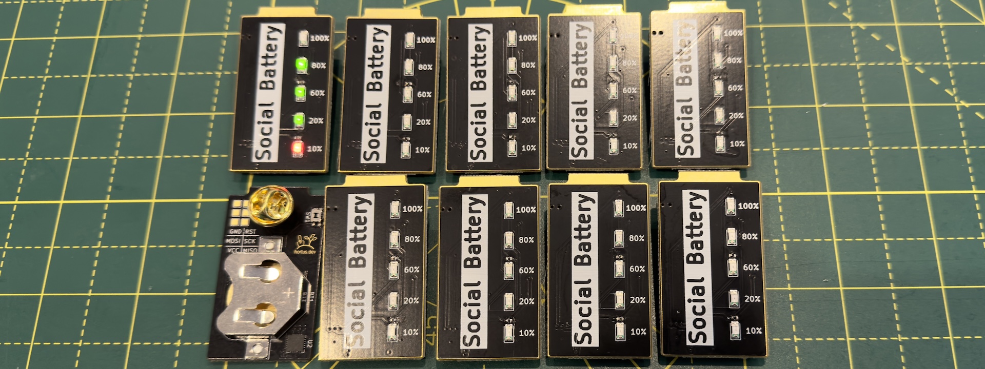 A few of the completed badges on my workbench
In the previous post in this series I recieved my prototypes and had a go at selling them online. With some succesful sales under my belt I felt confident enough to do a big small production run. I generated updated gerbers and placement files with the changes I had implemented after receiving my prototype boards. I uploaded them to JLC PCB and went through the process of configuring my order. I was planning to make 100, but I decided to tweak things a little to work out how quantity affected price and it turned out it wasn’t much more expensive to make 250 so I went with that. I also decided to go with ENIG for my surface finish rather than HASL. HASL finishes are achieved by dipping boards in molten solder and then removing the excess with ‘blades’ of hot air whereas ENIG is where copper surfaces are plated with gold. There are pros and cons with both methods. HASL is generally much cheaper, but ENIG results in a significantly more level surface which can be important when using components with lots of fine pitch pins. This isn’t really a problem for me but I decided to splash out for ENIG because I thought it would look nicer and probably be slightly harder wearing.
I also made sure that I had set up my components in KiCad so that it could generate a BOM that JLCPCB could automatically read and fulfil. This worked really well but sadly the ATtiny I needed was still not in stock with them. The did have the option to pre-order it, however. The lead time was about 2 weeks and the price was significantly cheaper than anything I could find through their global sourcing service, so I figured I’d accept the short wait in exchange for lower costs. Sadly it was too good to be true. A little while later I received an email asking me to pay the difference between the price initially shown and a new quote for my requested quantity of chips. The new price matched that of the cheapest global sourcing supplier so I wasn’t too surprised/upset - but it’s definitely worth bearing in mind that until all the components are in the warehouse and assigned to you there may be other costs.
The next wrinkle I ran into was surprisingly high shipping costs. I was expecting to pay quite a lot for shipping (in the region of £100) but the quote I was given was 5 times that. When I looked to see what was going on I realised that they had estimated the weight of my order to be 47kg which was definitely too high! It took a couple of attempts to get to the bottom of this but on the whole JLC support was extremely helpful. I was using the webchat and was surprised that I was almost instantly talking to real person who was actually able to fix issues with my order (or at the very least talk directly to the engineer handling it on my behalf). It turns out there a few things at play here:
- There is a concept called ‘volumetric weight’ which is actually just the volume that your shipment will occupy (in cubic cm) divided by 5000 which gets you ‘volumetric kilograms’. It seemed a bit ridiculous to me to jump through these hoops rather than just charging for, and calling it ‘volume’ but I realise now that it makes it easier to equate volume to weight and charge for whichever is going to be most expensive to carry.
- One of my components had an incorrect volume measurement recorded against it which was massively increasing the volumetric weight of PCB panels. This was quickly fixed by one of JLC’s engineers and that bought the costs down a fair bit.
- I’d got my numbers the wrong way around when configuring how I wanted my PCBs panellised. I’d asked for awkwardly long and narrow panel with 5x10 of my boards when what I really wanted a less awkward 10x5 panel. This was easily rectified by the engineer looking after my board though and saved me having to pay an additional fee for having an abnormally large board.
With all that sorted and out of the way all that was left to do was wait. In the end it took about two weeks to arrive. I was really pleased with the results apart from one thing… for some reason the LEDs looked really dim this time. Initially I assumed it was because I’d changed to slightly cheaper LEDs this time but that didn’t really make much sense. I double checked things and to my horror realised that I’d picked the wrong current limiting resistor for the LEDs… 330k Ohms rather than 330 Ohms. This was really irritating as it meant I had 500 0402 resistors to replace by hand. Very much doable but also really tedious! I’ve been working through these in batches as I’ve sold them and it’s not too bad but I wish I’d used larger resistors!
Apart from re-work the most tedious task that remained was programming. As mentioned in my previous post, I had planned for this by updating the board to be compatible with a pogo pin jig that I also designed. The board itself was a PCB manufactured again by JLC PCB (although this time I opted to do the assembly myself given that it only needed a regular pin header and some pogo pins) and a 3d printed guide to help align the pins with the contacts on the social battery PCB. This worked really well and it made programming a breeze! I should probably update it with slightly better tolerances so that it lines the pins up perfectly every time as it occasionally needs a tiny bit of jiggling to make a good connection - but to be honest I think it works well enough for now so I probably won’t bother.
Final thoughts
I started this project to see what JLC PCBs assembly service was like before committing to bigger, more complicated projects. I learned some important lessons that I will definitely use when designing my next project:
- This one feels obvious but it’s so easy to ignore - Always prototype and test your project on a breadboard (or similar method) before getting anything made. It doesn’t matter how simple the project is - the feedback loop is slow when it involves shipping things half way round the world, and even if it’s fiddly, you can save yourself a lot of time by just plugging some wires into a breadboard.
- Also probably quite obvious - but double check your component selections and don’t mess around with them between manufacturing runs unless totally necessary! When you’re making a significant number of boards, the consequences of making mistakes significant and will cost you money, time, or both!
- It’s worth identifying your hardest-to-obtain components up front - if you try and order dependant components at the same time and then discover that you can’t get your main component then you will be stuck with a bunch of possibly useless components in the JLC warehouse
- Don’t use small components for the sake of it. You hope that you won’t have to rework boards when your order arrives, but if you do have to you’ll thank yourself for choosing components that are easy to solder
Overall I’m really pleased with how this project has turned out. As of writing I’ve sold about a fifth of the badges that I made and whilst I’m not quite profitable yet (meta ads are eating into my margins) I should be soon. What’s really exciting to me is that there are total strangers out there who are enjoying (I hope!) something I’ve made.
If you want to get one for yourself then they are available for purchase at https://hortus.dev/products/social-battery
